Our Mission
Nano-Scale Research Center for Heterogeneous Integration Platforms (NSR-CHIP), led by Sandia National Laboratories, is a project funded by Department of Energy Office of Science that is part of the Microelectronics Science Research Centers.
Three centers will perform basic research in microelectronics materials, device & system design, and manufacturing science to transform future microelectronics technologies, focused on two technical areas, Energy Efficiency and Extreme Environments. It is one of 8 projects that are part of the Energy Efficiency MSRC called the Microelectronics Energy Efficiency Research Center for Advanced Technologies, or MEERCAT. NSR-CHIP is collaborating with other research institutions to head off a potential future energy crisis that could be driven in part by artificial intelligence.
As we look beyond Moore’s Law and challenges with scaling, we are running out of room as we get to an atomic level transistor. There is both a need and opportunity to redesign the microelectronics materials and innovation process.
Our Vision
Scientific Hypothesis
Understanding the interconnected fundamental interfacial properties (electronic, lattice, and thermal) of dissimilar 2D and 3D materials stacks within M3D HI structures will enable facile tunability of the properties (electronic, optoelectronic) of the constituent materials beyond traditional means of disparately engineering individual materials.
Research Operational Hypothesis
Closely coordinated, concerted collaboration and integration of the state-of-the-art resources of all the DOE NSRCs can develop and provide new capabilities tailored to the synthesis, integration, multimodal operando characterization, and machine-learning-based co-design frameworks towards system-level performance and efficiency enhancement, indispensable for realizing and accelerating the adoption of M3D HI.

Technical Thrust Areas
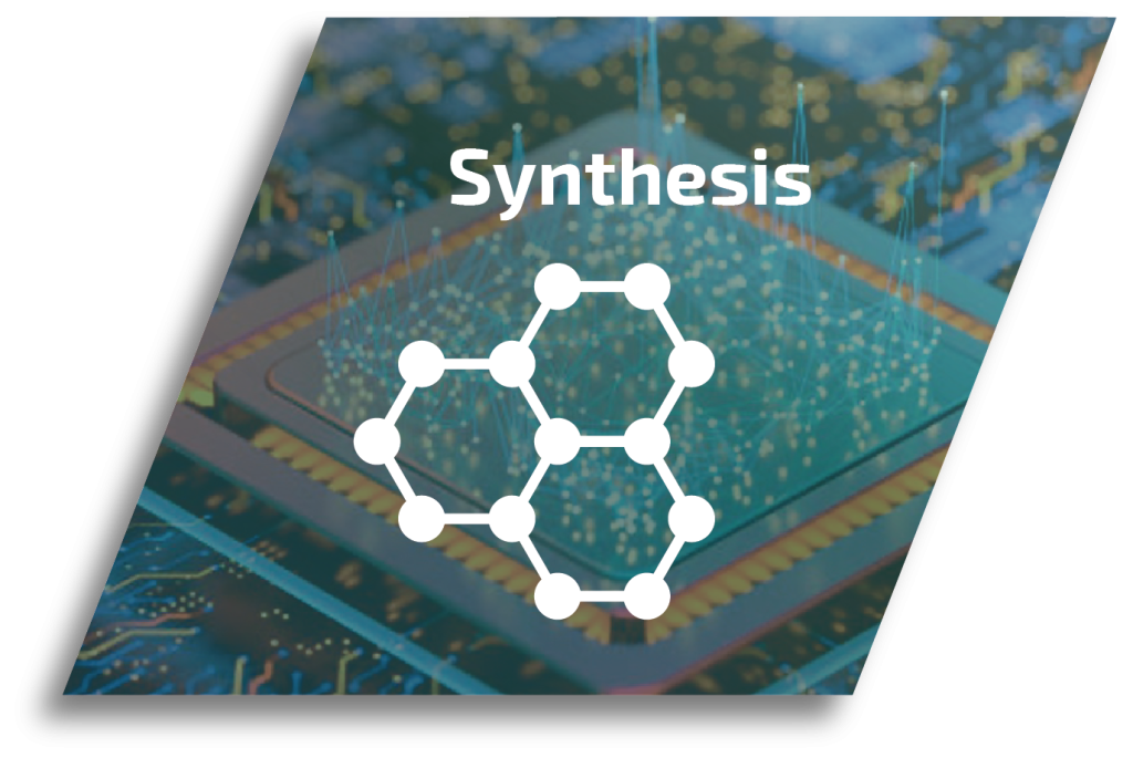
More About Synthesis
Goal: Establish the science foundation of advanced epitaxy methods and M3D HI stacking with controlled atomic defects, materials functions, and interface properties.
Expected Outcome: Complex heterogenous material structures, arrays, and interfaces.
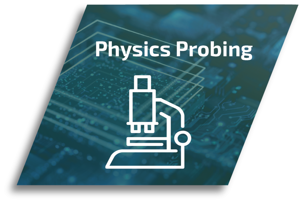
More About Physics Probing
Goal: Uncover the unique functional properties (electronic, transport, optical etc.) of M3D HI stacks of dissimilar materials systems (e.g., 2D on 3D materials) and the influences of atomic interfaces.
Expected Outcome: Interfacial properties, defect effects, and device behaviors.

More About Use Cases & ML Models
Goal: Utilize M3D HI in a system to demonstrate particle detection and employ a physics-informed machine learning framework to predictively connect multi-modal metrology and characterization data to system-level performance and energy efficiency.
Expected Outcome: Predictability between material properties and heterostructure behavior.
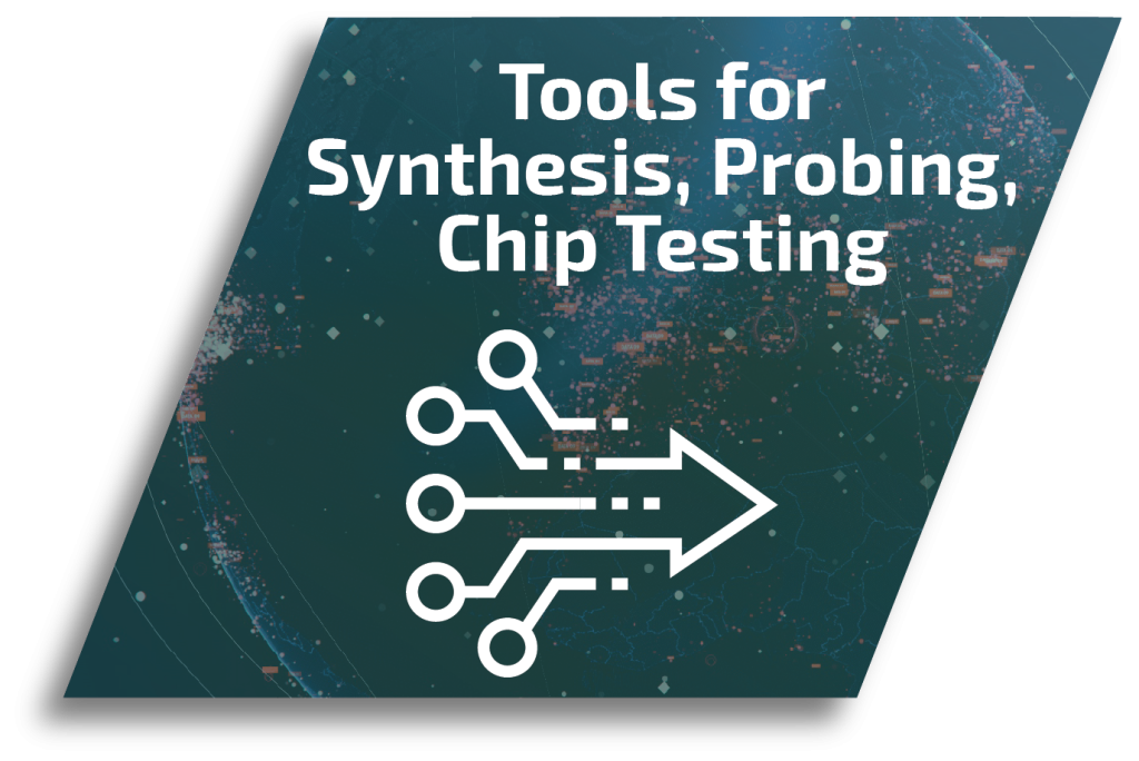
More About Tools
Goal: Develop a state-of-the-art multimodal M3D HI characterization framework for nondestructive operando metrology for buried materials and associated interfaces.
Our Collaborators
NSR-CHIP is a unique collaboration leveraging the DOE’s five scientific user facilities, called the Nanoscale Science Research Centers, along with partnerships with a few other institutions.


To learn more, please contact…

Jeffrey S. Nelson
Director, Center for Integrated Nanotechnologies (CINT)
NSR-CHIP Director
jsnelso@sandia.gov
office: (505) 284-1715
mobile: (505) 506-9485

Christian Mailhiot
Senior Manager, 8340 Materials Research
NSR-CHIP Associate Director
cmailhi@sandia.gov
office: (925) 294-2622
mobile: (925) 290-9606